PCB Parameters:
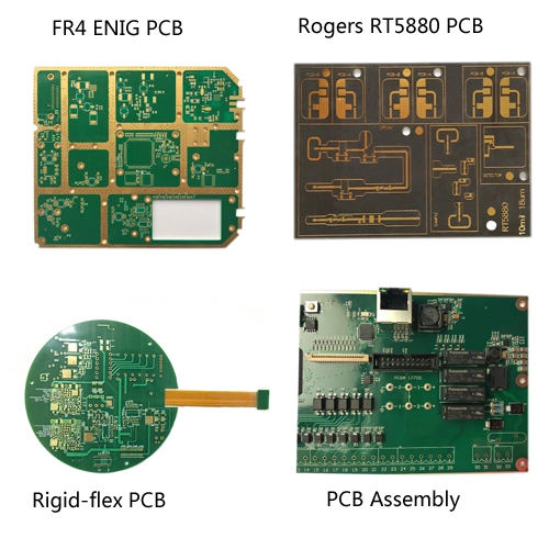
PCBs Products:
Testing Procedures For PCB Board:
We perform multiple quality assuring procedures before shipping out any PCB board. These include:
- Visual Inspection
- Flying probe
- Impedance control
- Solder ability detection
- Digital metallogenic microscope
- AOI (Automated Optical Inspection)
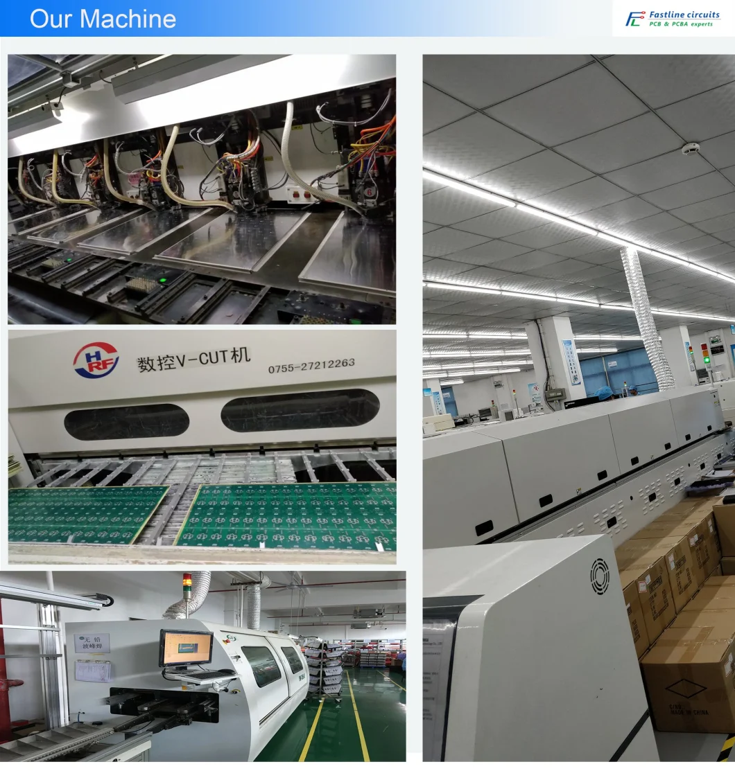
PCB manufacture machine:
Shipping Method and Payment terms:
1. By DHL, UPS, FedEx, TNT using clients account.
2.DHL, UPS, FedEx, TNT forwarder of China.
3. We could ship the parcel by Russia Special Air Line for
Russian customer
(No TAX in your there, 3 - 10 days to Moscow , 15-20 days to other city)
4. By sea or air for mass quantity according to customer's requirement.
5. By customer's Forwarder
6.Payment By Paypal,T/T,West Union,etc.
PCB Manufacture Capability
Company introduction:
Fastline Circuits Co.,Limited has the most diversified printed circuit board technologies available, including Single-sided PCB, Multilayer PCB, Aluminum based PCB, HDI PCB, Rigid-flex PCB, Flexible PCB, Heavy Copper PCB, Ceramic PCB, and PCB assembly and other special PCB boards.
We believe that the quality is the soul of an enterprise and provides time-critical, technologically advanced engineering and manufacturing services for the electronics industry.
Sound quality gains a good reputation for Fastline. Loyal customers has cooperated with us again and again and new customers come to Fastline to establish cooperation relationship when they hear of the great reputation. We look forward to offering high-quality service to you!
FAQ
Q1: What's your minimum order quantity?
A1: No MOQ , 1 pcs is accepted .
Q2: what file we should offer?
A2: PCB:Gerber file is better,( Protel ,power pcb,PADs file), PCBA : Gerber file and BOM list.
Q3:No PCB file/Gerber file, only have the PCB sample,can you produce it for me?
A3: Yes, we could help you to clone the PCB. Just send the sample PCB to us, we could clone the PCB layout and work out the PCB files, then produce for you.
Q4: What is the lead time?
A4:Sample needs 7-10 days, mass production needs 10- 15 days,
according to the order volume.Also we can provide quick time service 1-2days.
Q5: What payment terms do you have?
A5: For small orders, we usually prefer Paypal and Western Union; For bigger order,pls pay by TT.
| PCB SIZE | 170 x 64 |
| BOARD TYPE | Double sided PCB |
| Number of Layers | 2 layers |
| Surface Mount Components | YES |
| Through Hole Components | no |
| LAYER STACKUP | copper ------- 18um(0.5oz)+plate TOP layer |
| FR-4 0.7 mm | |
| copper ------- 18um(0.5oz)+plate BOT layer | |
| TECHNOLOGY | |
| Minimum Trace and Space: | 15 mil / 6.5 mil |
| Minimum / Maximum Holes: | 0.3 mm / 3.5 mm |
| Number of Different Holes: | 2 |
| Number of Drill Holes: | 35 |
| Number of Milled Slots: | 5 |
| Number of Internal Cutouts: | 0 |
| Impedance Control: | no |
| Number of Gold finger: | 0 |
| BOARD MATERIAL | |
| Glass Epoxy: | FR-4 Tg150ºC, er<5.4.IT-158, ITEQ Supplied |
| Final foil external: | 1 oz |
| Final foil internal: | 0 oz |
| Final height of PCB: | 0.8 mm ±0.08 |
| PLATING AND COATING | |
| Surface Finish | Selective hard gold on pads 10 u" |
| Solder Mask Apply To: | TOP and Bottom, 12micron Minimum |
| Solder Mask Color: | Matt blue, KSM-S6189BLM1 |
| Solder Mask Type: | LPSM |
| CONTOUR/CUTTING | Routing, v-cut |
| MARKING | |
| Side of Component Legend | TOP |
| Colour of Component Legend | White, IJR-4000 MW300, Taiyo brand |
| Manufacturer Name or Logo: | Marked on the board in a conductor and leged FREE AREA |
| VIA | Plated through hole(PTH), minimum size 0.3mm. |
| FLAMIBILITY RATING | UL 94-V0 Approval MIN. |
| DIMENSION TOLERANCE | |
| Outline dimension: | 0.0059" |
| Board plating: | 0.0029" |
| Drill tolerance: | 0.002" |
| TEST | 100% Electrical Test prior shipment |
| TYPE OF ARTWORK TO BE SUPPLIED | email file, Gerber RS-274-X, PCBDOC etc |
| SERVICE AREA | Worldwide, Globally. |
PCBs Products:
Testing Procedures For PCB Board:
We perform multiple quality assuring procedures before shipping out any PCB board. These include:
- Visual Inspection
- Flying probe
- Impedance control
- Solder ability detection
- Digital metallogenic microscope
- AOI (Automated Optical Inspection)
PCB manufacture machine:
Shipping Method and Payment terms:
1. By DHL, UPS, FedEx, TNT using clients account.
2.DHL, UPS, FedEx, TNT forwarder of China.
3. We could ship the parcel by Russia Special Air Line for
Russian customer
(No TAX in your there, 3 - 10 days to Moscow , 15-20 days to other city)
4. By sea or air for mass quantity according to customer's requirement.
5. By customer's Forwarder
6.Payment By Paypal,T/T,West Union,etc.
PCB Manufacture Capability
| Item | Manufacture Capability |
| Layers | 1-20 Layers |
| HDI | 2+N+2 |
| Material Types | Fr-4, Fr-5, High-Tg, Aluminum Based , Halogen Free, |
| Isola, Taconic, Arlon, Teflon, Rogers, | |
| Max. Panel Dimension | 39000mil * 47000mil (1000mm * 1200mm) |
| Outline Tolerance | ± 4mil (± 0.10mm) |
| Board Thickness | 8mil-236mil (0.2 - 6.0mm) |
| Board Thickness Tolerance | ± 10% |
| Dielectric Thickness | 3mil-8mil ( 0.075mm-0.20mm) |
| Min. Track Width | 3mil ( 0.075mm ) |
| Min. Track Space | 3mil ( 0.075mm ) |
| External Cu Thickness | 0.5 OZ - 10 OZ ( 17um - 350um) |
| Internal Cu Thickness | 0.5OZ - 6OZ ( 17um - 210um) |
| Drilling Bit Size ( CNC ) | 6mil-256mil ( 0.15mm - 6.50mm) |
| Finished Hole Dimension | 4mil-236mil(0.1mm - 6.0mm) |
| Hole Tolerance | ± 2mil (± 0.05mm) |
| Laser Drilling Hole Size | 4mil(0.1mm) |
| Aspect Ration | 16: 1 |
| Solder Mask | Green, Blue, White, Black, Red, Yellow, Purple, etc. |
| Min Solder mask Bridge | 2mil(0.050mm) |
| Plugged Hole Diameter | 8mil-20mil ( 0.20mm-0.50mm) |
| Beveling | 30o - 45o |
| V-scoring | +/-0.1mm, 15o 30o 45o 60o |
| Impedance Control | Min. 5% General ± 10% |
| Surface Finishing | HASL, HASL(lead Free), Immersion Gold |
| Immersion Silver, OSP, Hard Gold ( up to 100u" ) | |
| Certification | UL RoHS ISO9001: 2000 ISO14000: 2004 SGS |
| Testing | Flying probe, E-TEST, X-RAY Inspection , AOI |
| Files | Gerber Protel DXP Auto CAD PADS OrCAD Express PCB etc |
Company introduction:
Fastline Circuits Co.,Limited has the most diversified printed circuit board technologies available, including Single-sided PCB, Multilayer PCB, Aluminum based PCB, HDI PCB, Rigid-flex PCB, Flexible PCB, Heavy Copper PCB, Ceramic PCB, and PCB assembly and other special PCB boards.
We believe that the quality is the soul of an enterprise and provides time-critical, technologically advanced engineering and manufacturing services for the electronics industry.
Sound quality gains a good reputation for Fastline. Loyal customers has cooperated with us again and again and new customers come to Fastline to establish cooperation relationship when they hear of the great reputation. We look forward to offering high-quality service to you!
FAQ
Q1: What's your minimum order quantity?
A1: No MOQ , 1 pcs is accepted .
Q2: what file we should offer?
A2: PCB:Gerber file is better,( Protel ,power pcb,PADs file), PCBA : Gerber file and BOM list.
Q3:No PCB file/Gerber file, only have the PCB sample,can you produce it for me?
A3: Yes, we could help you to clone the PCB. Just send the sample PCB to us, we could clone the PCB layout and work out the PCB files, then produce for you.
Q4: What is the lead time?
A4:Sample needs 7-10 days, mass production needs 10- 15 days,
according to the order volume.Also we can provide quick time service 1-2days.
Q5: What payment terms do you have?
A5: For small orders, we usually prefer Paypal and Western Union; For bigger order,pls pay by TT.